- 您现在的位置:买卖IC网 > Sheet目录466 > KAC-9617 (Eastman Kodak Company)IC SENSOR IMAGE VGA 48CLCC
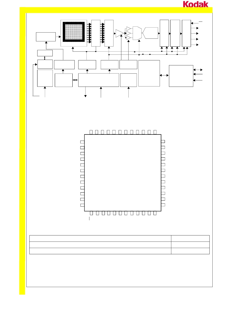
IMAGE SENSOR SOLUTIONS
Overall Chip Block Diagram
oe
R
d[11:0]
Row Address
Decoder
AMP
G
B
MUX 12 Bit A/D
pclk
hsync
POR
APS Array
vsync
Reset
Gen
Clock Gen
Row Address
Gen
Controller
(sequencer)
Vertical Horizontal
Timing Timing
Master Timer
Gain
Control
Power
Control
Register Bank
I 2 C Compatible
Serial I/F
sda
sclk
sadr
reset mclk
extsync
snapshot
pdwn
Figure 1. Chip Block Diagram
Connection Diagram
6
5
4
3
2
1
48 47 46 45 44 43
sclk
snapshot
resetb
pdwn
7
8
9
10
42
41
40
39
RSVD
pwl_ref
atest_in
atest_out
vss_dig
vdd_dig
hsync
vsync
pclk
mclk
d0
RSVD
11
12
13
14
15
16
17
18
KAC-9617
48 PIN LCC
38
37
36
35
34
33
32
31
offset
vdd_ana1
vss_ana1
vref_adc
vss_ana2
vdd_ana2
vss_od2
vdd_od2
1 9 2 0 2 1 2 2 2 3 2 4 2 5 2 6 2 7 2 8 2 9 3 0
Ordering Information
Description
KAC-9617
A small PCB that houses the KAC-9617 sensor together with all necessary discrete components.
KAC-9617IEA
KAC-9617HEADBOARD
www.kodak.com/go/imagers 585-722-4385
3
Email:imagers@kodak.com
发布紧急采购,3分钟左右您将得到回复。
相关PDF资料
KAC-9627
IC SENSOR IMAGE VGA 48CLCC
KB-A100SRW
LIGHT BAR 660NM RED 8.89X3.81MM
KB-B100SRW
LIGHT BAR 660NM RED 19.05X3.81MM
KB-C100SRW
LIGHT BAR 660NM RED 8.89X8.89MM
KB-D100SRW
LIGHT BAR 660NM RED 8.89X3.81MM
KB-E100SRW
LIGHT BAR 660NM RED 8.89X3.81MM
KB-F100SRW
LIGHT BAR 660NM RED 19.05X3.81MM
KB-G100SRW
LIGHT BAR 660NM RED 8.89X8.89MM
相关代理商/技术参数
KAC-9618
功能描述:IC SENSOR IMAGE VGA MONO 48-CLCC RoHS:是 类别:传感器,转换器 >> 图像,相机 系列:- 标准包装:480 系列:- 象素大小:6.7µm x 6.7µm 有源象素阵列:768H x 488V 每秒帧数:52 电源电压:3.3V 类型:CMOS 成像 封装/外壳:48-QFP 供应商设备封装:48-QFP 包装:托盘 请注意:* 配用:4H2105-ND - HEADBOARD FOR KAC-004014H2104-ND - KIT EVAL FOR KAC-00401 其它名称:4H20954H2095-NDKAC-00401-CBC-LB-A0
KAC-9618/HEADBOARD
功能描述:HEADBOARD FOR KAC-9618 RoHS:是 类别:编程器,开发系统 >> 过时/停产零件编号 系列:- 标准包装:1 系列:- 传感器类型:CMOS 成像,彩色(RGB) 传感范围:WVGA 接口:I²C 灵敏度:60 fps 电源电压:5.7 V ~ 6.3 V 嵌入式:否 已供物品:成像器板 已用 IC / 零件:KAC-00401 相关产品:4H2099-ND - SENSOR IMAGE WVGA COLOR 48-PQFP4H2094-ND - SENSOR IMAGE WVGA MONO 48-PQFP
KAC-9618EVAL-KIT
功能描述:KIT EVALUATION SENSOR KAC-9618 RoHS:是 类别:编程器,开发系统 >> 过时/停产零件编号 系列:- 标准包装:1 系列:- 传感器类型:CMOS 成像,彩色(RGB) 传感范围:WVGA 接口:I²C 灵敏度:60 fps 电源电压:5.7 V ~ 6.3 V 嵌入式:否 已供物品:成像器板 已用 IC / 零件:KAC-00401 相关产品:4H2099-ND - SENSOR IMAGE WVGA COLOR 48-PQFP4H2094-ND - SENSOR IMAGE WVGA MONO 48-PQFP
KAC-9619
功能描述:IC SENSOR IMAGE VGA 48-CLCC RoHS:是 类别:传感器,转换器 >> 图像,相机 系列:- 标准包装:480 系列:- 象素大小:6.7µm x 6.7µm 有源象素阵列:768H x 488V 每秒帧数:52 电源电压:3.3V 类型:CMOS 成像 封装/外壳:48-QFP 供应商设备封装:48-QFP 包装:托盘 请注意:* 配用:4H2105-ND - HEADBOARD FOR KAC-004014H2104-ND - KIT EVAL FOR KAC-00401 其它名称:4H20954H2095-NDKAC-00401-CBC-LB-A0
KAC-9619/HEADBOARD
功能描述:HEADBOARD FOR KAC-9619 RoHS:是 类别:编程器,开发系统 >> 过时/停产零件编号 系列:- 标准包装:1 系列:- 传感器类型:CMOS 成像,彩色(RGB) 传感范围:WVGA 接口:I²C 灵敏度:60 fps 电源电压:5.7 V ~ 6.3 V 嵌入式:否 已供物品:成像器板 已用 IC / 零件:KAC-00401 相关产品:4H2099-ND - SENSOR IMAGE WVGA COLOR 48-PQFP4H2094-ND - SENSOR IMAGE WVGA MONO 48-PQFP
KAC-9627
功能描述:IC SENSOR IMAGE VGA 48CLCC RoHS:是 类别:传感器,转换器 >> 图像,相机 系列:- 标准包装:480 系列:- 象素大小:6.7µm x 6.7µm 有源象素阵列:768H x 488V 每秒帧数:52 电源电压:3.3V 类型:CMOS 成像 封装/外壳:48-QFP 供应商设备封装:48-QFP 包装:托盘 请注意:* 配用:4H2105-ND - HEADBOARD FOR KAC-004014H2104-ND - KIT EVAL FOR KAC-00401 其它名称:4H20954H2095-NDKAC-00401-CBC-LB-A0
KAC-9627/HEADBOARD
功能描述:HEADBOARD FOR KAC-9627 RoHS:是 类别:编程器,开发系统 >> 过时/停产零件编号 系列:- 标准包装:1 系列:- 传感器类型:CMOS 成像,彩色(RGB) 传感范围:WVGA 接口:I²C 灵敏度:60 fps 电源电压:5.7 V ~ 6.3 V 嵌入式:否 已供物品:成像器板 已用 IC / 零件:KAC-00401 相关产品:4H2099-ND - SENSOR IMAGE WVGA COLOR 48-PQFP4H2094-ND - SENSOR IMAGE WVGA MONO 48-PQFP
KAC-9628
功能描述:IC SENSOR IMAGE VGA COLOR 48CLCC RoHS:是 类别:传感器,转换器 >> 图像,相机 系列:- 标准包装:480 系列:- 象素大小:6.7µm x 6.7µm 有源象素阵列:768H x 488V 每秒帧数:52 电源电压:3.3V 类型:CMOS 成像 封装/外壳:48-QFP 供应商设备封装:48-QFP 包装:托盘 请注意:* 配用:4H2105-ND - HEADBOARD FOR KAC-004014H2104-ND - KIT EVAL FOR KAC-00401 其它名称:4H20954H2095-NDKAC-00401-CBC-LB-A0
